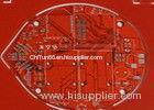
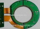
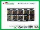
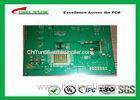
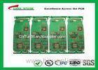
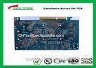
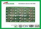
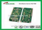
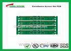
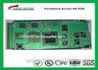
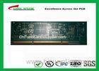
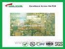
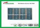
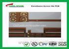
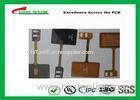
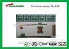
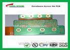
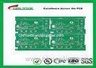
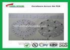
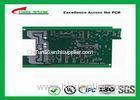
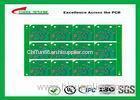
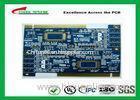
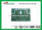
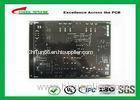
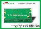
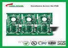
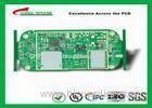
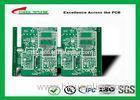
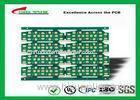
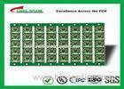
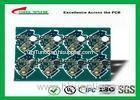
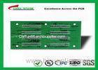
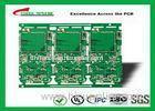
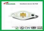
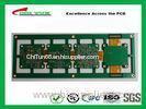
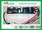
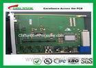
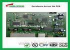
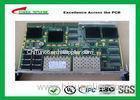
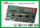
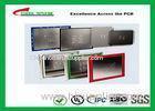
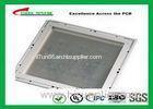
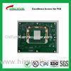
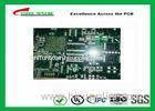
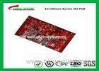
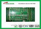
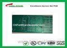
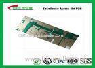
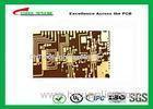
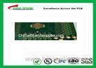
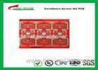
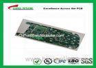
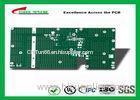
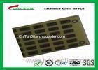
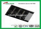
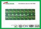
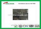
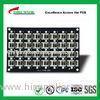
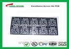
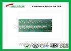
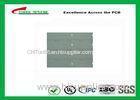
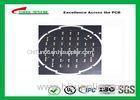
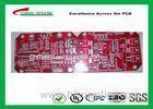
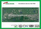
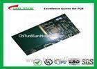
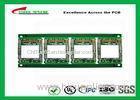
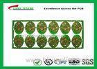
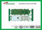
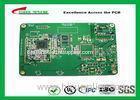
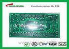
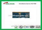
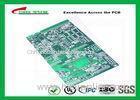
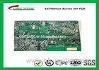
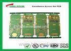
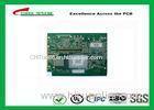
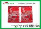
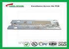
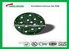
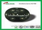
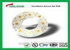
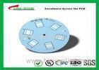
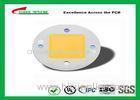
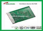
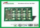
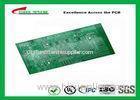
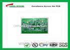
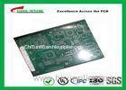
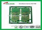
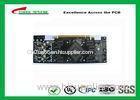
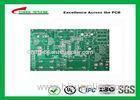
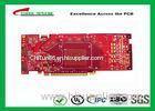
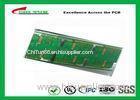
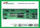
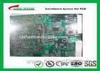
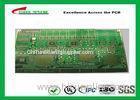
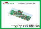
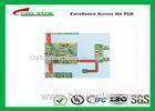
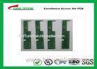
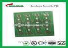
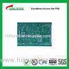
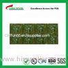
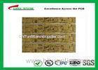
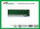
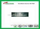
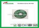
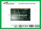
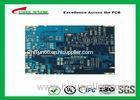
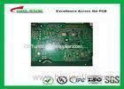
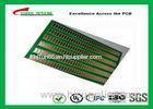
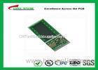
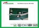
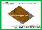
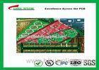
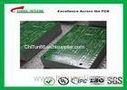
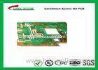
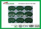
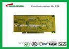
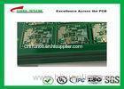
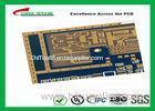
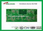
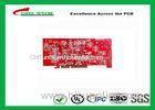
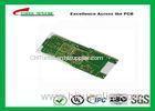
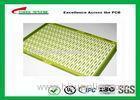
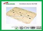
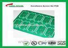
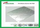
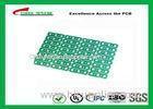
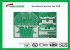
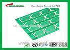
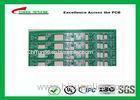
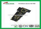
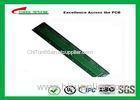
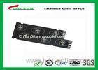
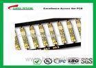
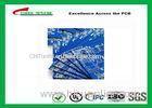
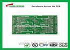
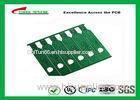
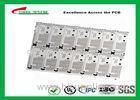
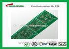
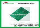
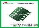
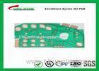
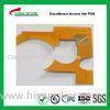
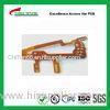
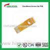
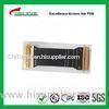
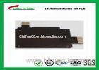
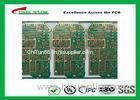
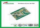
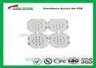
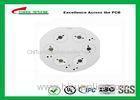
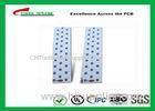
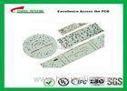
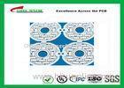
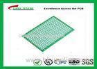
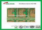
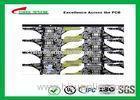
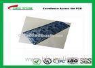
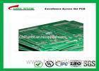
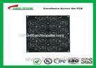
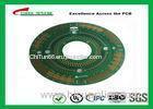
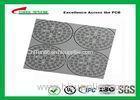
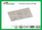
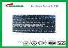
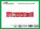
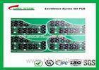
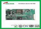
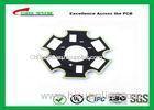
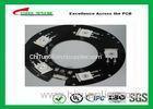
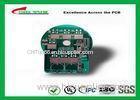
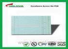
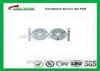
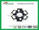
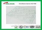
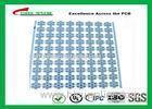
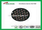
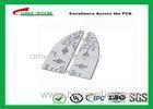
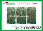
PCB Design And Fabrication PCB Engineering 6 Layer Hard Gold Surface Treatment
| Place of Origin: | Zhejiang, China (Mainland) |
|
|
|
| Add to My Favorites | |
| HiSupplier Escrow |
Product Detail
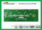
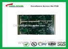
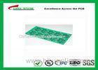
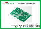
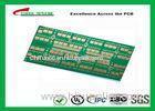
PCB Design And Fabrication PCB Engineering 6 Layer Hard Gold Surface Treatment
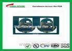
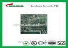
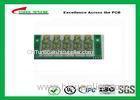
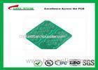
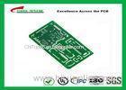
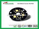
PCB Design And Fabrication PCB Engineering 6 Layer Hard Gold Surface Treatment
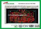
TECHNOLOGY:
. RoHS/ Lead Free
. HDI Microvias
. Blind Vias
. Buried Vias
. Selective Plating
. Impedance Control
Manufacturing Standard:
. IPC-A-600G Class II
. IPC-A-600G Class III
. PERFAG 2E for Double-Sided Board
. PERFAG 3C for Multilayer Board
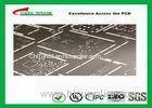
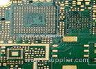
Capability
Min. Finished Holes Size: 0.008" (0.20mm)
Micro vias diameter: 0.004 TO 0.010 inches (0.10 - 0.25mm)
Minimum line width/spacing: 0.004/0.004 inches (0.10mm/ 0.10mm)
Maximum copper thickness: 5oz (140um)
Thin board thickness:
. DS - 0.008 inches (0.20mm)
. 4/L - 0.016 (0.40mm)
. 6/L - 0.020 inches (0.60mm)
Maximum board thickness:
. 275.8mil (7.0mm)
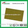
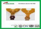
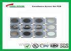
Surface treatment:
. HASL/lead free HAL/gold plating
. Immersion gold
. Immersion tin
. Immersion silver
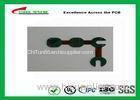
. Gold fingers (hard gold)
. OSP
Related Search
Find more related products in following catalogs on Hisupplier.com
Company Info
Chi Tun Electronics Co.,Ltd [China (Mainland)]
Business Type:Manufacturer
City: Shenzhen
Province/State: Guangdong
Country/Region: China (Mainland)